
This blog was originally published on April 2, 2018.
Relentless pressure to reduce mainframe expenditures and the close correlation between CPU consumption and software expense (in both traditional peak four-hour rolling average licensing models and even more so for the increasingly prevalent consumption models where all CPU is chargeable) have combined to make CPU reduction initiatives a key focus area across IT organizations.
This is the final article in a four-part series focusing on the prominent role processor cache efficiency plays in CPU consumption. The three previous articles can be accessed below:
- Part 1: Lower MLC Software Costs with Processor Cache Optimization
- Part 2: How Optimizing LPAR Configurations Can Reduce Software Expense
- Part 3: Optimizing MLC Software Costs with Processor Configurations.
Previous articles in the series have shown that a significant portion (30-50%) of all CPU cycles on current z processor models are spent waiting for instructions and data to be staged into Level 1 processor cache so they can be executed, highlighting the importance of understanding key cache concepts and having good visibility into the excellent metrics that are available. This article examines changes in processor cache design for the z14 and z15 processor models.
A significant change in hardware manufacturing technology was introduced with the z13 processor, shifting from multi-chip modules (MCMs) to single-chip modules (SCMs). While achieving the desired reductions in manufacturing costs and power consumption, it also introduced a non-uniform memory access (NUMA) topology that is accompanied by more variability in latency times for cache accesses.
This explains why processor cache efficiency now plays a much more prominent factor in CPU consumption on z processors. In contrast to the revolutionary change introduced with the z13, the z14 and z15 models reflect evolutionary changes.
Since we are unlikely to see sizable improvements in machine cycle speeds going forward, expect processor cache efficiencies to play a major role in the increases in capacity delivered by newer generations of z processors, as is indeed the case with z14 and z15 processors.
z14 and z15 Cache Design Changes: Overview
The rationale and impact of these significant cache changes will be examined in the rest of this article. Most of these changes were introduced with the z14. Any z15-specific changes will be noted.
- A unified Level 4 cache enables point-to-point access to remote drawers.
- Important changes to the PR/SM LPAR algorithms were made to reduce cache waiting cycles.
- Several increases to cache sizes at various levels of the hierarchy were implemented.
- The Level 1 Translation Lookaside Buffer (TLB) was merged into Level 1 cache.
Unified Level 4 Cache
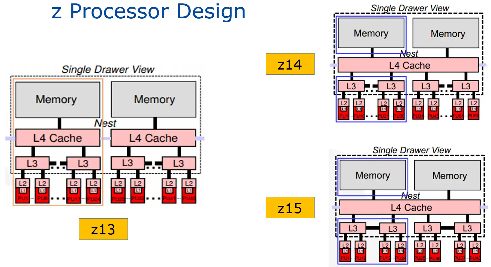
Figure 1: z Processor Design (IBM)
Figure 1 shows drawer cache hierarchy diagrams for z13 (left) and z14 and z15 (right). In Levels 1 through 3, all three models are largely similar. But one very significant change from the z13 to the following models is the unified L4 cache. This plays a key role in the increased capacities delivered by the z14 and z15. The rationale for this change is to reduce the cost of “remote,” cross-drawer accesses.
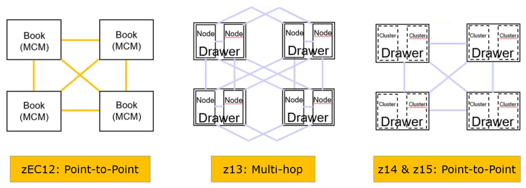
Figure 2: Drawer Interconnect Technologies (IBM)
Figure 2 compares the drawer interconnect technologies for recent z processors. zEC12 (and prior models) provided point-to-point connectivity between all “books” (now drawers), enabling accesses to remote cache to be reached directly.
But on the z13, depending on the node in which the data resides, remote accesses could now require multiple hops, often requiring hundreds of machine cycles. This is one key factor explaining why LPAR topology plays such a major role in Finite CPI on the z13, and why some high RNI workloads had performance challenges migrating to z13 processors. The z14 and z15 design unifying L4 cache restores point-to-point connectivity between all the L4 caches. Thinking of the travel time saved by taking nonstop flights (z14 and z15) as opposed to connecting flights (z13) will make the value of this improvement readily apparent.
PR/SM Algorithm Changes
Partnering with the unified Level 4 cache that reduced the cycles required by cross-drawer accesses, significant changes were made to PR/SM algorithms to reduce the frequency of those remote accesses. These algorithm changes are particularly noteworthy:
- One change prioritizes the effort to fit an LPAR within a single drawer, seeking to reduce the frequency of expensive remote accesses. The increase from eight cores per chip on the z13 to ten (z14) or twelve (z15) makes this more achievable by increasing the size of an LPAR that will now fit within a drawer.
- Another change prioritizes placing General Purpose logical CPs (GCPs), Vertical Highs (VHs) and Vertical Mediums (VMs), in close proximity on the same chip or cluster. This is in contrast to the z13, which prioritized collocating VHs for both GCPs and zIIPs. This frequently occurred at the expense of VM GCPs, which wound up located in a separate drawer, especially on large LPARs.
- In addition, on the z15 PR/SM seeks to optimize LPAR placement down to the CP chip boundary, introducing additional efficiencies.
Case Study 1: Reduction in Finite CPI Penalty
When PR/SM placed VM logical CPs in a different drawer from the VHs for that LPAR (a common occurrence for large LPARs on z13 processors), this often created a sizable Finite CPI penalty for work executing on those VMs. (You may recall from Article 1 that Finite CPI quantifies machine cycles spent waiting for data and instructions to be staged from processor cache or memory into L1 cache.) This penalty occurred because many of their cache accesses travelled across drawers—very expensive in terms of machine cycles on the z13.
As we have seen, the unified L4 cache and PR/SM algorithm changes were designed to reduce the magnitude of that Finite CPI penalty. This case study quantifies the impact of those changes at one site.
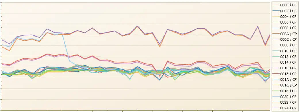
Figure 3: Finite CPI By Logical CP—z13
Figure 3 presents the Finite CPI by logical CP for a large LPAR when it was running on a z13. Note the very significant penalty for the VMs and VLs (along the top of the chart) compared to the VHs. Large LPARs on z13 processors frequently incurred a substantial Finite CPI penalty where the LPAR topology located VMs and VLs in a separate drawer from the large number of VHs.
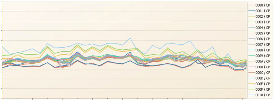
Figure 4: Finite CPI By Logical CP—z14
Figure 4 displays the significant change when this LPAR migrated to a z14, significantly reducing the Finite CPI penalty for the VMs and VLs.
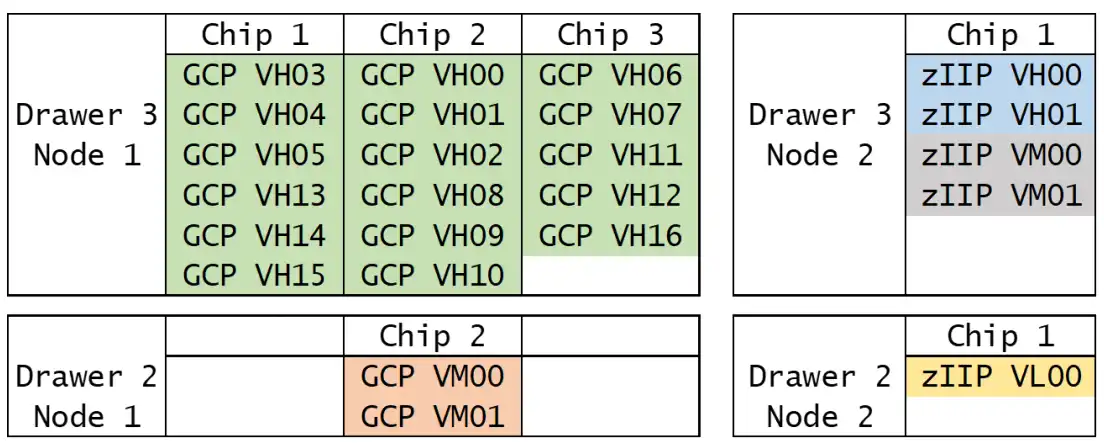
Figure 5: LPAR Topology—z13
Diagrams of the underlying LPAR topologies on the z13 and z14 confirm that the previously described changes in the PR/SM algorithms had their desired outcomes. When this LPAR was running on the z13 (Figure 5), the VMs (in orange) were in a separate drawer (Drawer 2) from all the VHs (in green, in Drawer 3). This led to frequent expensive cross-drawer accesses by the VMs.
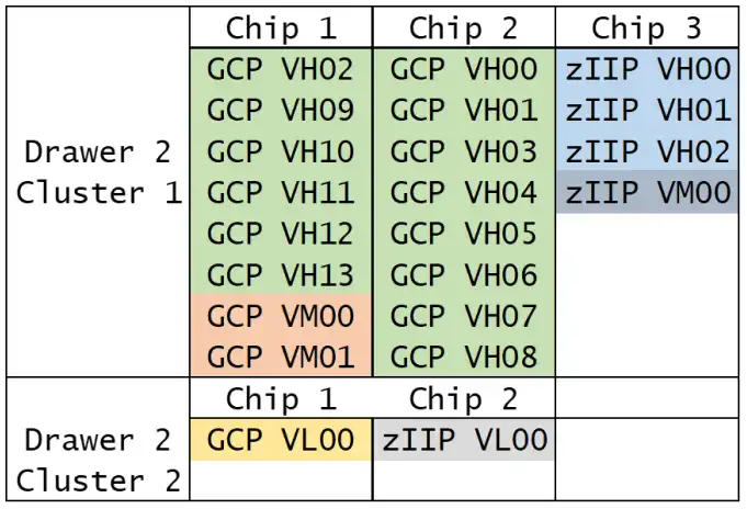
Figure 6: LPAR Topology—z14
Figure 6 shows the changes to the topology after this LPAR migrated to the z14. Now the VMs (in orange) and VHs (in green) reside in the same drawer and even share the same L3 cache. In fact, PR/SM was able to configure the entire LPAR (GCPs and zIIPs) in a single drawer.
The outcome of this case study provides evidence that the PR/SM algorithm changes had their intended effect, dramatically reducing the Finite CPI penalty for VMs and VLs because of improved proximity in the LPAR topology.
Cache Size Increases
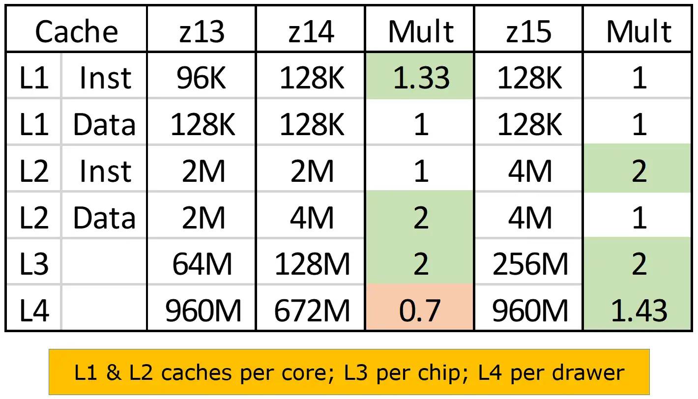
Figure 7: z13/z14/z15 Cache Sizes
Several cache size increases were delivered by both the z14 and z15, captured in Figure 7. Level 1 instruction cache became one-third larger, Level 2 data and instruction cache sizes both doubled, and Level 3 cache also doubled.
Constraints in processor chip real estate limit the opportunities for increased cache sizes. It is likely IBM leveraged its machine level instrumentation to deploy these increases in the tiers of the cache hierarchy where they would have the biggest overall benefit for reducing cache misses and resulting accesses to subsequent levels of cache and memory.
Level 1 TLB Merged into Level 1 Cache
The final design change listed earlier was that the Level 1 Translation Lookaside Buffer (TLB1) control information has been merged into Level 1 cache. The TLB performs the critical and high-frequency function of translating virtual addresses into real addresses. Now beginning with the z14, the Level 1 cache contains all the data needed to perform that address translation function, eliminating the need for a separate TLB1 and the potential for any TLB1 misses.
Again, metrics from z14 and z15 implementations show very good results from these TLB design enhancements, typically reducing the total CPU consumed by TLB misses by more than half.
Case Study 2: Impact on Delivered Capacity with z13 to z15 Upgrade
Now let’s review a case study showing the impact on delivered capacity of an upgrade from a z13 to a z15, with special focus on the impact on processor cache efficiency and the role cache metrics play in explaining the results. Though it represented an 11% capacity increase, this z13-722 to z15-719 upgrade spanning two model generations still resulted in a reduction of three physical CPs, leading to fewer VHs.
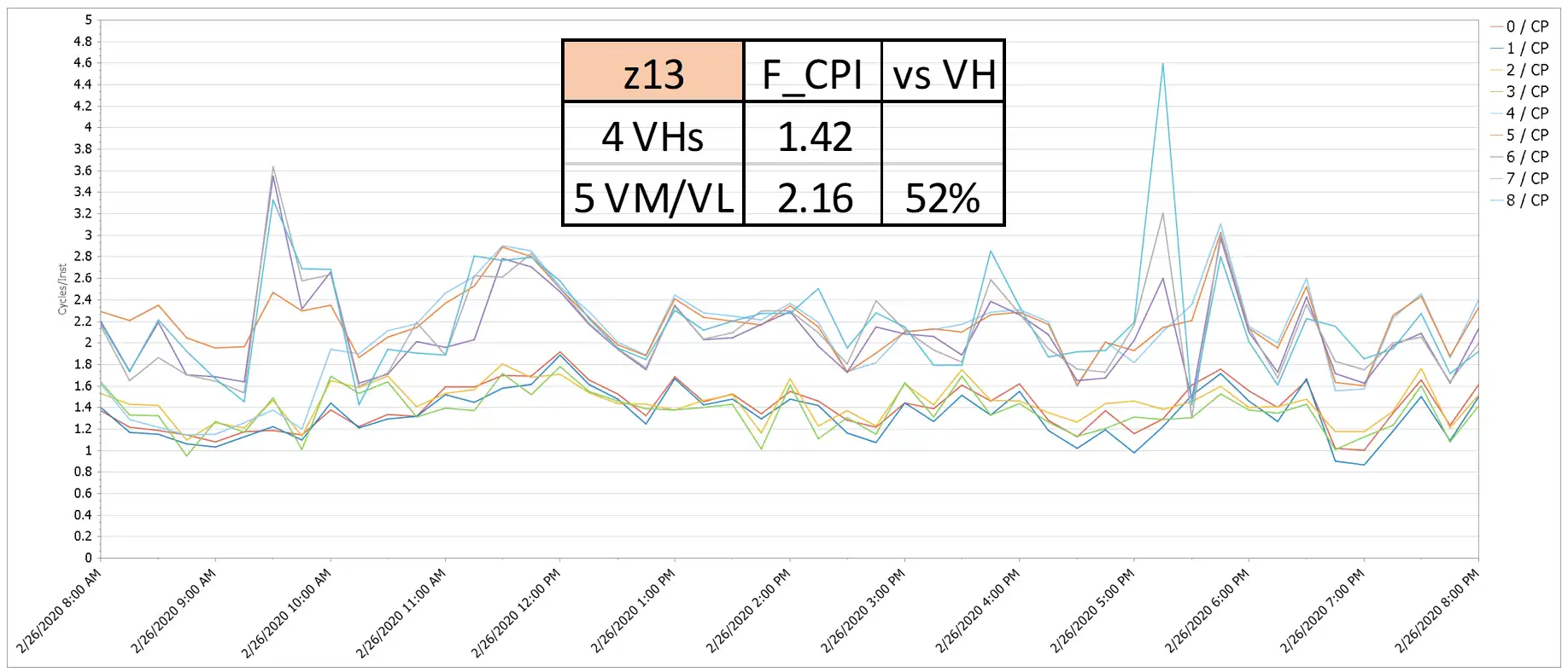
Figure 8: Finite CPI by Logical CP – z13
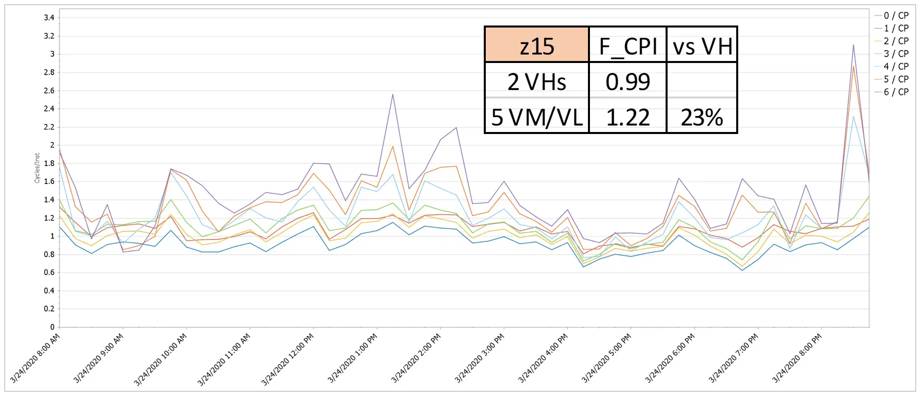
Figure 9: Finite CPI by Logical CP – z15
When running on the z13, a large LPAR in this environment had a Finite CPI penalty of 52%, as seen by the big gap in Finite CPI values between the four VH and the five VM/VL logical CPs in Figure 8. When that LPAR moved to the z15, that penalty was significantly reduced as is visually apparent in Figure 9. It is likely the PR/SM algorithm change mentioned earlier that places a greater priority on closer proximity between the VHs and VMs contributed to this improvement.
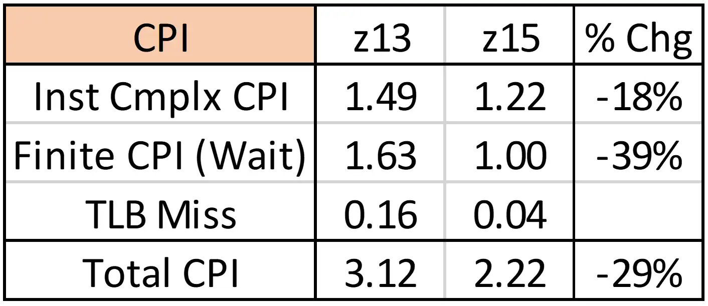
Figure 10: z15 Impact on CPI Components
Figure 10 presents the reductions in Cycles per Instruction (CPI) resulting from the upgrade. This business workload realized an 18% benefit from instruction architectural improvements across the two generations, but the cache enhancements created an even bigger reduction of 39% in waiting cycles.
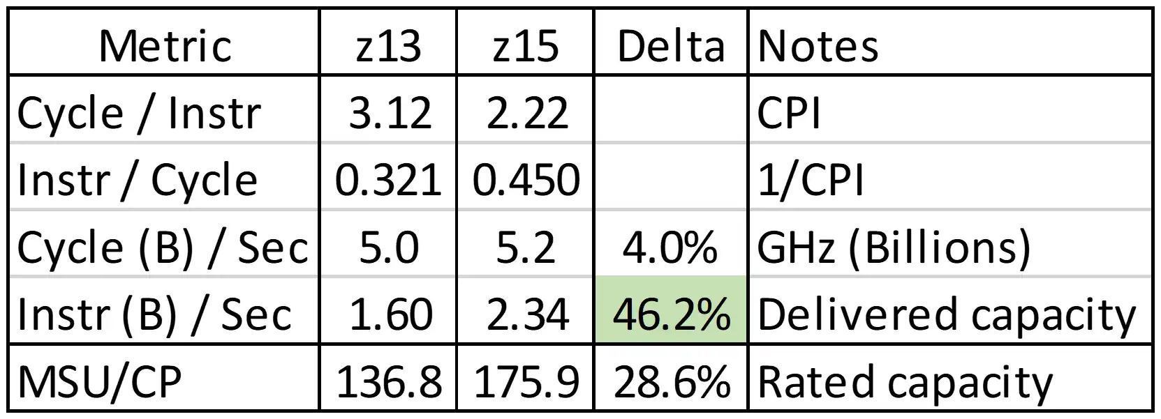
Figure 11: z15 Impact on Delivered Capacity
Finally, Figure 11 translates this CPI improvement into a 46% increase in delivered capacity that far exceeded the 29% in rated capacity between the two models, resulting in a sizable reduction in total MSU consumption. The workload in this example that was previously experiencing a sizable Finite CPI penalty while running on a z13 especially benefitted from the cache enhancements delivered with the z15.
Summary
This series of articles has demonstrated that processor cache performance plays a more prominent role than ever before in the capacity delivered by processors beginning with the z13. The zEC12 and earlier era where processor speed improvements “covered a multitude of sins” and mainframe performance analysts could get by with ignoring processor cache metrics is gone, at least for the foreseeable future.
Sites thinking strategically will increasingly factor CPU efficiency and software expense considerations into their hardware configuration planning.
Another trend that continues in full force is that software expense continues to consume a growing percentage of the overall mainframe budget, while hardware costs represent an ever-smaller percentage. Considering these factors, these articles have encouraged readers to re-examine the traditional assumption of mainframe capacity planning that running mainframes at high utilizations is the most cost-effective way to operate. Sites thinking strategically will increasingly factor CPU efficiency and software expense considerations into their hardware configuration planning.
Finally, this series of articles has sought to help performance analysts realize the importance of having a solid understanding of and clear visibility into key processor metrics. Armed with this understanding and visibility, analysts may often identify opportunities to achieve significant CPU and software expense savings by leveraging those metrics to optimize processor cache. Hopefully, the methods presented to reduce Finite CPI and CPU consumption, and the case studies confirming the effectiveness of these methods in real-life situations, have equipped readers with the ability to identify and implement optimizations that will improve the efficiency, competitiveness, and long-term viability of the mainframe platform in their environments.
Sources
[Havekost2020] Todd Havekost, “Lessons on Optimizing Processor Cache from z15 Upgrade Case Studies”, IntelliMagic zAcademy Session #5, May 2020.
[Hutton2019] David Hutton, “IBM Z Microprocessor Optimization Primer,” SHARE, March 2019.
[Hutton2020] David Hutton, “The RNI-based LSPR and The IBM z15 Performance Brief,” SHARE Session #26997, February 2020.
How to use Processor Cache Optimization to Reduce z Systems Costs
Optimizing processor cache can significantly reduce CPU consumption, and thus z Systems software costs, for your workload on modern z Systems processors. This paper shows how you can identify areas for improvement and measure the results, using data from SMF 113 records.
This article's author
 Todd Havekost
 Share this blog
Related Resources
Why Am I Still Seeing zIIP Eligible Work?
zIIP-eligible CPU consumption that overflows onto general purpose CPs (GCPs) – known as “zIIP crossover” - is a key focal point for software cost savings. However, despite your meticulous efforts, it is possible that zIIP crossover work is still consuming GCP cycles unnecessarily.
Top ‘IntelliMagic zAcademy’ Webinars of 2023
View the top rated mainframe performance webinars of 2023 covering insights on the z16, overcoming skills gap challenges, understanding z/OS configuration, and more!
Making Sense of the Many I/O Count Fields in SMF | Cheryl Watson's Tuning Letter
In this reprint from Cheryl Watson’s Tuning Letter, Todd Havekost addresses a question about the different fields in SMF records having different values.
Book a Demo or Connect With an Expert
Discuss your technical or sales-related questions with our mainframe experts today